Introduction
In many applications, analog voltages are involved, and the actions of the microcontroller should depend on a given analog voltage level (for example a data logger). In order to convert it into a digital value (i.e. a binary number), analog to digital converters (ADCs) are used. The ADC compares the measured voltage to a reference voltage. The resulting number will be the ratio of the measured voltage and the reference voltage, where a ratio of 1 or greater would be mapped to the highest possible 10-bit value (0b1111111111), and 0 or smaller would be mapped to the lowest value (0b0000000000). The ATMEGA8 has an integrated 10-bit ADC that is connected to 6 of the pins in the DIP package (marked red in the following picture). Here I present a small setup and some C code that demonstrates how the ADC can be used.
Setup
A schematic drawing of the setup is shown in the next picture. Relevant pins of the ATMEGA are labeled. The connections to the programmer (also serving as power supply) are shown in blue. Note that the programmer can stay connected all the time and will not interfere with the operation of the circuit.
There are 3 sources for the ADC reference voltage for the ATMEGA8: the supply voltage, a voltage provided at the AREF pin, or an internal 2.56V reference.
I will use the internal reference. In this case a capacitor has to be connected tot the AREF pin. If you build that circuit, I encourage you to disconnect that capacitor and see what happens to the output: it will be completely random.
Firmware
As always, making use of the ADC requires to write the correct values to the right registers, and as always, everything is well documented in the ADC section of the datasheet. The following program will measure the voltage from a variable resistor divider with the ADC and use the value to switch some LEDs that will show the binary representation of the measured ADC value.

The program will do the ADC setup and enter an infinite loop, in which it measures the voltage at ADC5 pin and displays the value on the LEDs. The LED on pin PC3 has the most significant bit of the 10-bit value, and PB0 has the least significant bit.
ADCSRA |= (1<<ADEN);
The voltage reference is selected by the two bits REFS1 and REFS0 in the ADMUX register. Table 74 on page 199 of the datasheet shows, that both bits have to be set in order to get the internal voltage reference.
ADMUX |= ( (1<<REFS1) | (1<<REFS0) );
Since I connected my analog signal to ADC5, the number 5 has to be written to the MUX[0:3] part of the ADMUX register
ADMUX |= 5;
A conversion is started by setting ADSC bit to 1 in the ADCSRA register. If the conversion is done, the ADC sets this bit back to 0.
ADCSRA |= (1<<ADSC);
while(ADCSRA & (1<<ADSC)); // wait until conversion is done
uint16_t value;
value = ADCL;
value |= (ADCH<<8);
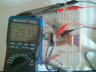
Finally, some pictures of my setup, showing three different settings of the voltage divider. A multimeter is connected to the ADC input voltage to verify the ATMEGA8 measurement. The 10-bit value can be seen on the right hand side with the least significant bit on the lowest LED and the most significant bit on the top LED.


The complete program
#include <avr/io.h>
#define F_CPU 1000000UL  // 1 MHz
#include <util/delay.h>

int main(void)
{
  // enable ADC
  ADCSRA |= (1<<ADEN);
  ADMUX |= ( (1<<REFS1) | (1<<REFS0) ); // internal reference
  ADMUX |= 5;                           // select ch. 5 (pin ADC5)

  // LED setup
  // PORTB[0:5] as output
  DDRB  = 0x3f; // 0011 1111
  // PORTC[0:2] as output
  DDRC  = 0x0f; // 0000 1111

  for (;;)
  {
    uint16_t value;

    ADCSRA |= (1<<ADSC);        // start single measurement
    while(ADCSRA & (1<<ADSC));  // wait until measurement done

    // read result bytes (low and high)
    value  = ADCL;
    value |= (ADCH<<8);

    // display number
    PORTB = value;
    PORTC = value>>6;
  }
}
Finally, some pictures of my setup, showing three different settings of the voltage divider. A multimeter is connected to the ADC input voltage to verify the ATMEGA8 measurement. The 10-bit value can be seen on the right hand side with the least significant bit on the lowest LED and the most significant bit on the top LED.


Keine Kommentare:
Kommentar veröffentlichen